All About 4 Layer PCBs
Obtaining a full understanding of what 4 layer PCBs are as well as how they function and where they are used isn’t as complicated as it may sound. PCBs or printed circuit boards are the backbones of many modern electronics such as cell phones, computers, toys, electronic exercise equipment, wearable tech, and more. The fact is, printed circuit boards play a much larger role in our day-to-day lives than we may realize especially with the advancements in technology making them smaller, faster, durable, and even flexible!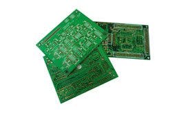
But what makes a 4 layer printed circuit board different from a 2 layer or even a 6 layer? In this article, we’ll go over the design process of a 4 layer printed circuit board as well as the main differences between a 2 layer PCB and a 4 layer PCB. Read along and find out what the specific use for a 4 layer PCB is.
What Is A 4 Layer PCB?
The wonderful and aptly named 4 layer printed circuit board is an integral electronic component that utilizes multiple conductive pathways from different onboard components such as resistors, capacitors, transistors, sensors, and more to output electrical signals. One of the main advantages of a 4 layer circuit board is that wires are no longer needed, this is because the four copper layers allow for multiple routing pathways as well as power. Additionally, this allows for 4 layer circuit boards to be smaller in size allowing for integration in smaller and more complex devices such as smartwatches.
Unfortunately, 4 layer printed circuit boards does have some disadvantages including expense and difficulty reconfiguring circuits in the inner layers if need be. Because of these downsides, they aren’t always the best option for simpler projects. However, it is fair to argue that the advantages that come with a 4 layer printed circuit board outweigh the disadvantages. With the progression of technology and electronics, it’s possible we’ll see some of these weaknesses slowly diminish.
Designing A 4 Layer PCB
The design process of a 4 layer printed circuit board can get fairly complex due to the intricacies of optimal component placement, pathway forming, and circuit routing. It takes a special skill set to be able to prepare expert-level printed circuit board designs and configurations and with the addition of multiple layers, it takes the design process to the next level.
High-level circuit board engineers begin designing printed circuit boards by taking into consideration what the circuit board needs to accomplish. Where and when electric currents need to be sent as well as size limitations. After the purpose of the circuit board is understood, architects use specific computer-aided design (CAD) software to build a prototype of each layer of the desired circuit board. This crucial design step will make or break the outcome of the produced circuit board so architects have a high level of attention to detail.
These schematics are then sent off to be printed onto a photo film which will then be transferred onto circuit board blanks that are coated with a photosensitive substance that allows for the printed design to be quickly displayed onto the blank. This is done for each layer before the 4 layers are etched and engraved by machines and then pressed together. After this, components are added to the board and quality inspections take place. Then the board is thoroughly tested for ideal function.
4 Layer PCB Vs 2 Layer
There are many key differences between the 4 layer printed circuit board and the 2 layer printed circuit board as far as function and production go. In this section, we’ll cover some of the differences in both aspects of these two wonderful electronic essentials.
To begin, the obvious difference between the two is the number of copper layers within each board. The 2 layer PCB (or double-sided PCB) contains two layers that are copper coated on both the top and bottom of the board with an insulating layer made of substrate material in between the two copper plates. While the 4 layer PCB contains four copper layers with a substrate material in between each layer. Any printed circuit board with more than two layers is considered a “multilayer” circuit board.
2 layer PCBs can be found in residential HVAC systems, printers, amplifiers, and other computer peripherals.
4 layer PCBs and other multilayer PCBs can be found in more complex electronics such as cell phones, space equipment, medical imaging equipment, and satellite systems.
Here are some of the advantages and drawbacks of both the 4 layer printed circuit board and the 2 layers (or double-sided) printed circuit board.
2 layer circuit board (Advantages)
- Lower production costs – because of fewer intricacies in manufacturing
- Design flexibility – allows for larger use
- Density – great for home appliances
- Quicker production time – lower complexity, not as many layers need to be produced
2 layer circuit board (Disadvantages)
- Not ideal for heavier currents
- Not the best choice for more complex projects
- Lower tolerance to heat
- Lower power threshold
4 layer circuit board (Advantages)
- Durability – due to the number of layers
- Lightweight – because internal wiring is not necessary
- Size – typically compact and used in many devices
- Versatile – can be used in simple or more advanced technologies
4 layer circuit board (Disadvantage)
- Higher cost – because of additional materials
- Longer production time – due to involute production
- Difficult repairs – accessing inner layers for repairs is complicated
The top and bottom surface layers of 4 layer PCBs are intended as layers for signal. Additionally, the inner couple of layers is for ground and supply. The numerous layers in a 4 layer printed circuit board allow the board to handle more power than a 2 layer due to its density and capacity for higher temperatures.
If you’d like to learn more about the differences between the 4 layer printed circuit board and the 2 layer printed circuit board as far as the production and design process go, feel free to pick up the phone and give our friendly team at Avanti Circuits a call. We will provide you with valuable information and help guide you to choose the right PCB for your project.
Contact Us Today For A Free Estimate
We hope we were able to educate you about the 4 layer printed circuit board, its uses, design process, and difference from a 2 layer printed circuit board. If you need additional information as to the number of layers you may need for your printed circuit board project or prototype, don’t hesitate to reach out and contact our team toll-free today as well as obtain a free estimate on our multilayer printed circuit board manufacturing service. We are eager to be your partner and supplier in the printed circuit board industry!
We appreciate you for taking the time to learn more about our passion and hope to hear from you soon.
Phone Numbers:
- Phoenix area: 602 866 7227
- Toll Free Phone: 888 595 8876
- Phoenix area fax: 602 375 1909
- Toll Free Fax: 800 234 7731
Hours:
- Monday: 8 AM 5 PM
- Tuesday: 8 AM 5 PM
- Wednesday: 8 AM 5 PM
- Thursday: 8 AM 5 PM
- Friday: 8 AM 5 PM
- Saturday: Closed
- Sunday: Closed