All About The Multilayer PCB Fabrication Process
Here at Avanti Circuits, we can help you with your multilayer PCB needs. We have been in this exciting industry for almost 40 years and we’re experts in the multilayer PCB fabrication process.
Multilayer printed circuit boards are quite different from regular ones. This means they need to be designed and manufactured well. Offering the user much more flexibility and reliability, you need a manufacturer who can give you exactly what you need. We know that we can help you with this, ensuring you’re perfectly happy with every single multilayer PCB you receive.
We will be happy to talk with you about your design and your circuit board specifications. Contact us today at (602) 866-7227 and let us help you.
What Are Multilayer PCB’s?
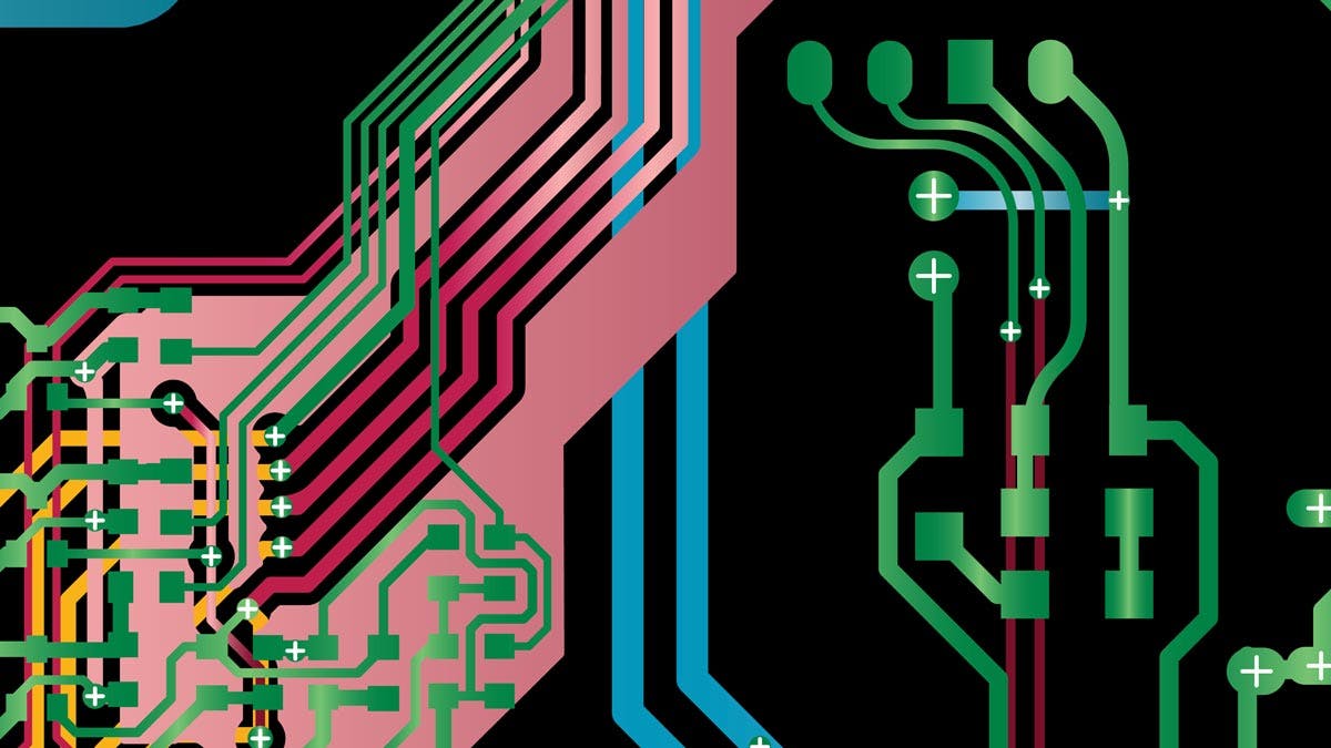
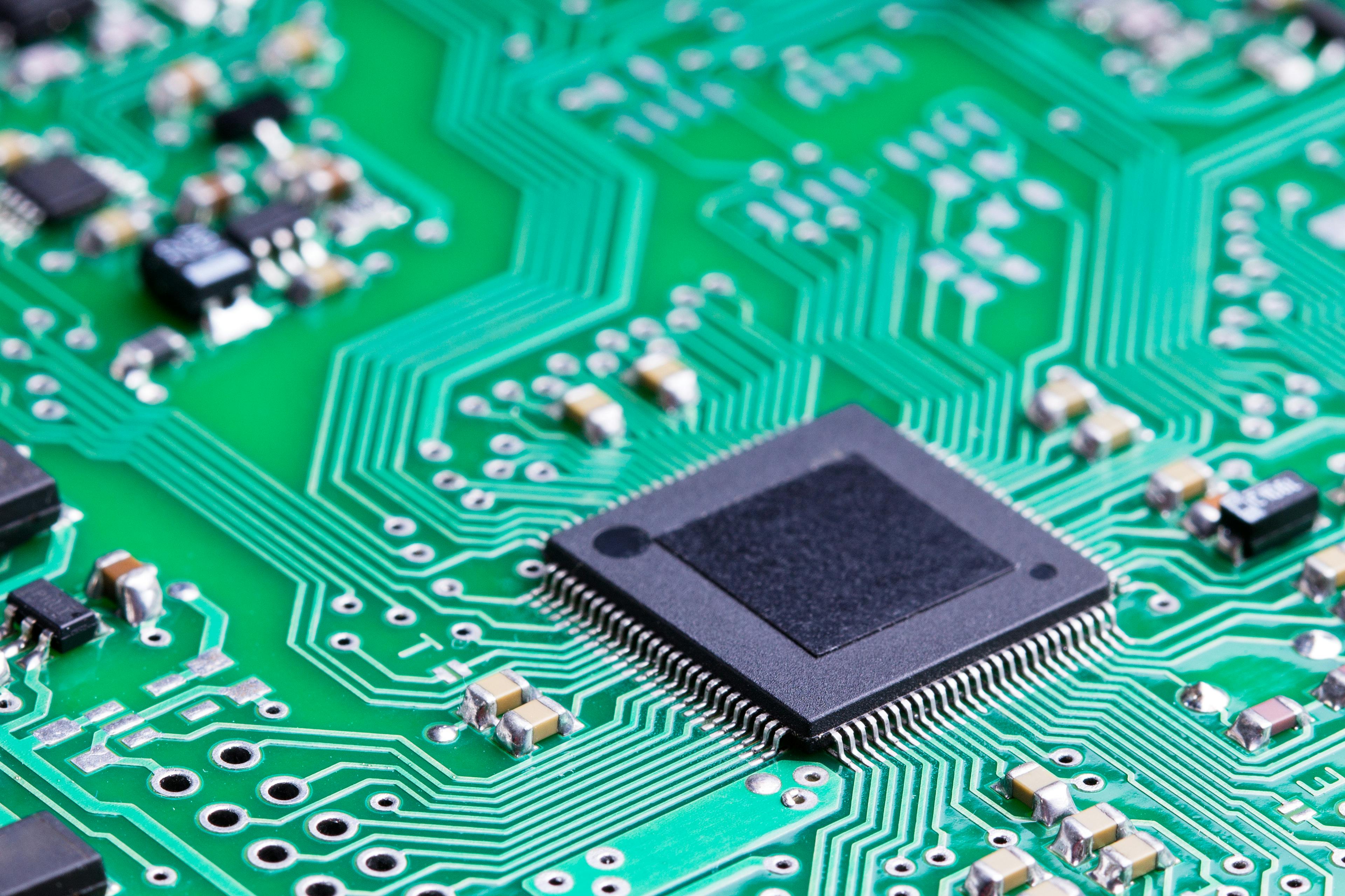
A multilayer printed circuit board is similar to regular printed circuit boards. However, they come with multiple layers, typically at least 3. In addition to this, multilayer printed circuit boards are stronger than regular PCBs. In addition to this, users can find that they are better at saving space and they offer a lot of flexibility.
Multilayer PCBs have at least one conductor pattern inside the board itself. This feature works to increase the area that is available for wiring. 4 and 8 layer printed circuit boards are commonly used. This is because they have just the right amount of complexity for a range of purposes. However, there is always the capacity to add more layers, but it depends on the device it is housed in. Some smart phones can use a PCB with up to 12 layers, thanks to the demands that the circuit has.
Most multilayer printed circuit boards have an even number of layers. This is because an odd number of layers can cause issues such as twisting or warping once they have been soldered. In addition to this, having an odd number of layers comes with no cost savings. This is because odd-numbered PCBs are not the typical or standard type of PCB to make. The manufacturer will need to take extra time to create an odd number of layers.
– Identifying a multilayer PCB
There are a few ways for you to identify a multilayer PCB. One of the first things you can do is to shine a light onto the board’s edge. When you do this, you may see some signal traces. However, they will only light up if the copper is close to the PCBs edge. You could also use a bright light to determine whether you can see any inner layers. Shine the light where there aren’t any plans or traces on the outer layers. You could also look for individual layers as some manufacturers label them.
– Common uses for a multilayer PCB
Multilayer printed circuit boards are commonly used in a range of devices. This includes:
- Computers
- Cell phones
- GPS technology
- Heart Monitors
- X ray equipment
– What you need to know
Multilayer PCBs can cost a little more than regular PCBs. However, they are much more flexible and reliable. The manufacturing time tends to be longer, but this is simply because there are more layers to work with. Do not worry, if you need a fast turn around multilayer printed circuit boards, we can help you.
Repairs can also be more complex when you use this type of PCB. However, all of our circuit boards are checked once they come off the production line. We want to make sure that they are of a very high quality for you. We also want to make sure that there are no issues when we send them to you. We check every single circuit board that we make. We know that you have high standards and this is just one of the ways that we give you what you need.
How Are Multilayer PCB’s Fabricated?
When it comes to fabricating multilayer printed circuit boards, layers of prepeg are used. Prepeg is a form of fabric reinforcement that has had a resin system already pre-impregnated. When they’re ready to be turned into multilayer PCBs, the prepeg is laminated under high temperatures and pressures. This process ensures there is no air trapped between the layers. Any conductors that are found on the PCB are locked in by resin, which is an adhesive. The resin works to hold every single layer together. Every layer is then cured and melted.
– Range of materials
A range of materials is used to create this type of printed circuit board. They can range from epoxy glass, Teflon materials, or even ceramic.
Multilayer printed circuit boards can contain:
- One layer of copper foil
- One layer of prepeg
- Another layer of copper foil
- One layer of printed circuit board core
- One layer of copper foil
- One layer of prepeg
- An additional layer of copper foil
PCB core and prepeg are very similar. The difference is that prepeg isn’t fully cured. What this means is that it’s easier to change its shape.
The different layers of core, prepeg, and foil are all added to a lamination press. High temperatures and high pressure is applied. This causes the prepeg to begin to melt. When this occurs, all of the layers are joined together very effectively. Once the PCB has been left to cool, there is a solid multilayer PCB that can be used in a variety of ways.
Equipment Required For Multilayer PCB Manufacturing
Here at Avanti Circuits, we always use high performance printed circuit board equipment. We want to work with equipment that ensures we always manufacture PCBs that are of a very high quality.
The manufacturing process is a complicated one that requires a lot of skill. This is where our experts come in and make a real difference in the manufacturing process.
Some of the equipment that we use includes:
- Drilling machine – This machine creates a range of cavities and slots in a circuit board. It does this before any components have been mounted onto it. The cavities and slots are created by a drill bit that is smaller than any of the components that will be used. An electrolytic etching technique is used to remove any material from the hole.
- Pattern plating line – This equipment masks off the copper surface. It only plates the pads and traces in accordance with the circuit pattern.
- Multilayer pressing equipment – This machine works by using heat and pressure to bond all of the PCB layers together.
- Solder mask exposure machine – A layer of solder mask that is photosensitive is sprayed on all sides of each panel. The ink is cured right away.
- Pattern expose machine – Once the required etching is undertaken, the PCB is exposed to light that projects the pattern of the printed circuit board.
- Solder mask develop line – After the PCB has been developed, openings are then created in the pattern. Components can then be soldered onto copper pads.
- Legend/solder mask oven – Solder mask is used because it is a well-known protective coating. It can help to prevent accidental bridging while also protecting the board from the environment. An oven is used to ensure the solder mask has a dry, firm surface.
- Pattern plating line – This process involves using an electrochemical process. During the process, a metal is placed on the circuit board’s surface. It’s also added to the plated through-holes. The plating process typically uses copper.
- Strip film/etching/strip tin line – This part of the manufacturing process involves removing unwanted copper from the printed circuit board. More specifically, the non-circuit copper is removed. This ensures that the required pattern is achieved.
- PCB material cutting machine – A PCB material cutting machine is manufactured to make cutting very easy. Some machines are full of blades, others cut printed circuit boards using lasers.
- PTH Line – A plated through hole line is used to drill holes from the top of the circuit board through to the bottom. This allows the added components to make direct contact with their conductive layers.
- Solder mask silk print machine – A machine such as this prints the LPI (Liquid photo imageable) solder onto the printed circuit board.
- Solder mask scrubbing line – At this stage of the manufacturing process, the unwanted solder is removed or “scrubbed” from the line. This ensures that only the required solder mask stays on the PCB.
- Pattern plating line – Here is where the pattern is set onto the PCB. The copper surface is masked off and the traces and pads are plated. The pattern outlines where the solder mask and components should sit. This allows those on the manufacturing line to make sure everything is exactly where it needs to be. Any deviation from the plating line could result in the PCB failing to work as well as it should, if at all.
- V-cut machine – Also known as “v-scoring” and “v-grooving”, this procedure cuts a “v”-shaped groove onto both the top and the bottom of the printed circuit board. This is so that any circuit board can be split relatively easily. However, the v is the right depth to ensure that the smallest amount of material can be left in place so the boards stay together should they need to.
- PCB E-test machine – We always test our PCBs as soon as they have been manufactured. We do this because we think it’s the right thing to do. Your multilayer circuit board will be tested using an adapter E-test machine or a flying probe. This is one of the only types of machine that will pick up broken and incorrect conductors. Any manufacturer that fails to use this type of machine risks sending their customers defective PCBs.
- AOI machine – An automatic optical inspection machine is used to detect even the smallest problems and defects on your printed circuit boards. A camera is used to autonomously scan for missing components and quality issues. Again, any manufacturer that fails to use this type of machine risks sending their customers defective PCBs.
We use a wide range of printed circuit board equipment. Using only equipment that we trust ensures that we can continue to manufacture PCBs to a very high standard.
Why Choose Our Multilayer PCB’s?
All of our multilayer PCBs have been expertly manufactured. Our team of experienced manufacturers is here to ensure every single multilayer PCB that you receive is of a very high quality. Did you know that we check every PCB that we manufacture? We do this to make sure that every PCB you receive is high quality and it works well. We work this way because we know this is what you would want from us.
In addition to this, you should choose our multilayer PCBs because they:
- Have better flexibility when compared to a single layer PCB
- Have power and ground layers that are placed in such a way that they offer better EMI shielding
- Contain easier control impedance
- Are smaller than many multilayer PCBs. This means they can be used in more devices
- Save you space when compared to single or double-layer printed circuit boards
- Have a much higher assembly density
- Lower the number of PCBs that aren’t very strong
We have been working in this industry for almost 40 years, and we’re proud of this. A American-owned business, we take pride in all that we do. All of our printed circuit boards are made in the USA, and we always ensure we’re perfectly happy with every PCB we send your way.
Our multilayer printed circuit boards are used in many different industries such as:
- The medical industry
- The military
- The automotive industry
- The aerospace industry
It’s absolutely crucial that every PCB that is manufactured by us works the way it should. It needs to be high quality, trustworthy, and built to last.
We can also offer you the following:
- Competitive pricing – Here at Avanti Circuits, we offer all of our customers the most competitive pricing you will find in this industry. You will not come across any additional charges or hidden fees. We believe in being completely upfront with you about our pricing because we think it’s the best way to be.
- Guaranteed quality – We always stand behind the work that we do. We have a lot of knowledge and expertise, allowing us to meet all of your PCB needs. We can even meet your most demanding standards and specifications.
- Great customer service – Our management team has more than 200 years of combined experience. When you want the experts to manufacture your PCBs, you should come to us. We can speak with you about your design and your circuit board specifications. We are here to help you.
- Fast turnarounds – From time to time, you may need to make use of our fast turnaround service. We know that you need some PCBs quicker than others. Do not worry. We can work with your time sensitivities. We have an excellent track record of meeting all of our deadlines and keeping all of our commitments.
- Low minimums – Do you need low production or prototype quantities? We can help you with this.
- Diverse capabilities – Our capabilities are nothing short of diverse. We can manufacture the multilayer printed circuit boards that you need. We can also manufacture PCBs that are high density or have exotic finishes or counts. Talk to us today.
- Corporate values – Our corporate values ensure that we always work with uncompromising honesty. We also work with integrity in all that we do.
All of the above advantages allow us to be successful. The printed circuit board manufacturing market has experienced a closure of almost all US-based manufacturers. Just 30 years ago there were more than 2,500 manufacturers in this country. Now they are few and far between.
We have been in this industry for almost 40 years, and we’re proud that we’re still here. We can be your go-to for all of your long-term and immediate PCB needs.
CONTACT US TODAY FOR A MULTILAYER PCB CONSULTATION
Here at Avanti Circuits, we can help you with your multilayer PCB needs. We know more than a thing or two about the multilayer PCB fabrication process and we can help you. Whether you need a fast turnaround, low minimums, exotic materials, or a team that’s reliable, we can help you. We have been in this industry for almost 40 years, and we’re confident that we can give you exactly what you are looking for.
We will be happy to talk with you about your design and your circuit board specifications. Contact us today at [(602) 866-7227](tel:(602) 866-7227) for a multilayer PCB consultation.