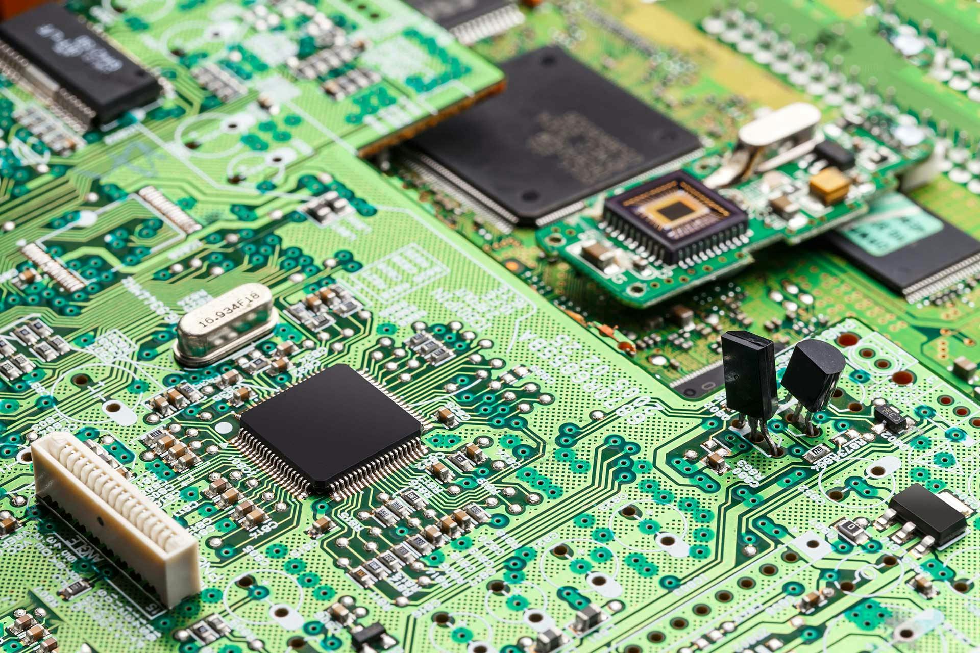
Large PCB Board Manufacturing
Here at Avanti Circuits, we are proud to manufacture a large PCB board for you. We know that you need high-quality, reliable large PCBs that work well. This is where we can help you. With 39 years of experience in this industry, we know what it takes to provide all of our customers with exactly what they’re looking for. Whether you are one of our well-known customers or a first-time customer with a small business, we can help you.
You can trust this American business to fulfill all of your large PCB board manufacturing requirements. Contact us today at 602-375-1909 so that we can manufacture exactly what you are looking for. We’re here to help you. Get in touch today.
What To Consider When Making Large PCB’s
Any printed circuit board that is more than 12 inches wide is typically considered to be a large PCB. Large PCBs can occasionally be hard to manufacture as they have limitations that are set by their sheer size.
Below, you can find some of the considerations you need to be aware of when making large PCBs.
- High layer count – The higher the layer count is, the more specialized the manufacturer is. This is because many manufacturers tend to offer 2-4, or 6-10 layers. Some do offer 12 or more layers, but they can be very specialized. In addition to this, the more layers you need, the slower the manufacturing process will be.
- Quick-turn processes – Not all manufacturers are capable of producing quick-turn PCBs that are large. This is because the amount of copper needed for traces, the high-speed design, and the impedance control can impact the manufacturing process.
- The thermal impact – The sheer thickness of the ground planes and their power can have a significant impact on the solder and the soldering process. The more metal that there is on the board, the more solder and heat is required. As a result, it could take a lot longer for the solder reflow profile optimization to be defined.
- The price – Typically, when you order more PCBs, the cost of the individual board will be lower. However, if you were to order large printed circuit boards, the cost per board (or unit) won’t be lower. This is because large PCBs do not fit in the panels that are traditionally used when manufacturing boards.
- The number of connectors – When many connectors are used on a backplane, much more work is needed to be undertaken to connect the pins and make sure that they work well. This can lead to much longer test times.
All of these factors need to be taken into consideration when a manufacturer is making large printed circuit boards. Please feel free to get in touch with us if you have any questions about the above considerations or anything else. We want you to have large PCBs that work well and do exactly what you need them to do. We’re a friendly team that is here to help.
Designing Your Large PCB Layout
Large printed circuit boards can be hard to design. This is because it can be difficult to route all of the traces without them coming into contact with each other. However, for now, we are going to concentrate on designing the layout so you can understand it a little more.
- Create the schematic – The schematic is a blueprint for your PCB. It shows you the components used, how they are connected, and the relationship between them. Converting a schematic to a board is much easier than designing on a board.
- Create a blank printed circuit board layout – Now it’s time to set the layer stack up, dimensions, and circuit board shape. If you don’t wish to do this now, it can be done at a later stage. Please let us know if you have any queries about the layer stack. We may be able to help you.
- Link the schematic to your PCB – Make sure that the schematic and PCB layout are interlinked so you can access them at the same time. Be sure to verify or save any changes you have made at this stage. Saving the changes now will mean you won’t need to go through the process again.
- Designing the PCB stackup – Define the shape and layer stackup of your PCB. At this stage, you may need to choose from a range of laminates and materials for your PCB. If you are new to the world of PCB design, this stage can seem a little overwhelming at first.
- The design rules – Here is where the sheer number of design rules may, again, overwhelm you. Many different PCB design programs have an extensive number of categories. It is unlikely that you will need to use all of the design rules for your designs. Any rules that you do use should be used with consideration to the tolerances and specifications of your manufacturer’s equipment.
- Placing the components – Some programs allow you to place your chosen components automatically or manually. Just make sure that your PCB is laid out well.
- Inserting the drill holes – Before you even think about routing your traces, you should place all of your drill holes. If you have a complicated design, you might need to change it a little at this stage.
- The route traces – As soon as you have placed all of your components, you can route your traces. Make sure you keep the process as simple as possible to avoid confusion.
- Adding the labels and identifiers – Once your PCB layout has been verified, you can add a logo, identifiers, labels, or imagery to your printed circuit boards. Use reference identifiers for your components. This will help with the assembly process. Be sure to also include polarity indicators as well as pin 1 indicators, and any labels that can prove to be helpful. Please feel free to talk to us about any images and logos that you want to use. This is to ensure you always use fonts that are easily readable.
- Generating the design files – Always verify the layout of your circuit board. Run a DRC (Design rule check) if you can. You could do it automatically using your chosen program or manually, should you prefer. As soon as the board has passed the DRC, you should generate the files for us. The files will need to include all of the information we need to build your large printed circuit boards. Be sure to add any data, special requirements, or information that could assist us in the manufacturing process.
Materials Used
Materials used in PCBs can include:
- Copper
- Silkscreen
- Soldermask
- Substrate
Other materials that are used include:
- BT, MS, PI, and PPO as a special material base class
- Epoxy resin (FE-3, FR4, FR5) as a paper base class or glass fiber cloth base class
- PF resin (FR1, FR2, XPC) as a paper base class
- Polyester resin as a paper base class
- UL94-V0 and UL94-V1 as a flameproof type
- UL94-HB is a non-flameproof type
The materials used in the manufacturing of a large printed circuit board may differ depending on our preferred materials and your design. Please contact us if there are any materials you would specifically like us to use.
About Our Large PCB Manufacturing Process
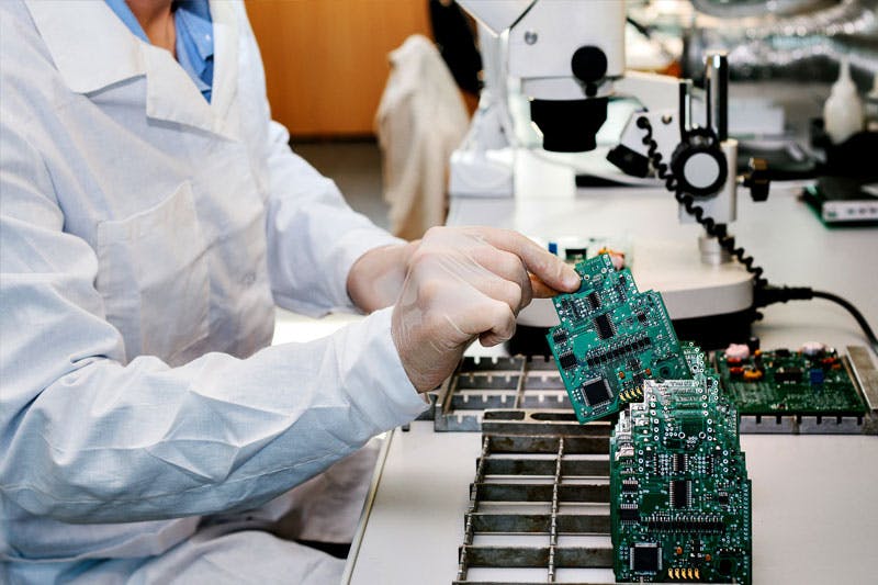
When you ask us to manufacture a large printed circuit board for you, you can trust us to do the job properly. We are here to help you give your customers the best possible PCBs.
Before we agree to manufacture your large PCBs, we will take a look at your design. We want to make sure that every PCB we make is of the highest standard. If we find an issue with your design, we will contact you. We will make you aware of the issue so that it can be corrected.
When this process is complete, we will begin manufacturing your large pcb. Did you know that we check each and every printed circuit board that we make? We want to ensure that you always receive a high-quality PCB from us, no matter how many you have ordered. Whether you order 500 or 5,000 it’s important that every PCB works well for you. If we find a fault in any of the PCBs during our stringent quality checks, we will resolve the issue. We take this step very seriously as we know you’d want us to.
CONTACT US TODAY FOR A PCB MANUFACTURING CONSULTATION
Here at Avanti Circuits, we are proud to be able to manufacture the right large pcb board for you. No matter what industry you’re in or why you need a large printed circuit board, we can help you.
You can trust this American-owned business to fulfill all of your large PCB board manufacturing requirements. Contact us today for a PCB manufacturing consultation at 602-375-1909 so that we can give you exactly what you are looking for. If you’re located outside of Phoenix, AZ, call us toll free on 888-595-8876. We’re here to help you with all of your large PCB needs. Call us today.